- 您现在的位置:买卖IC网 > Sheet目录2006 > LTC2630HSC6-LZ12#TRPBF (Linear Technology)IC DAC 12BIT R-R SC70-6
LTC2630
6
2630ff
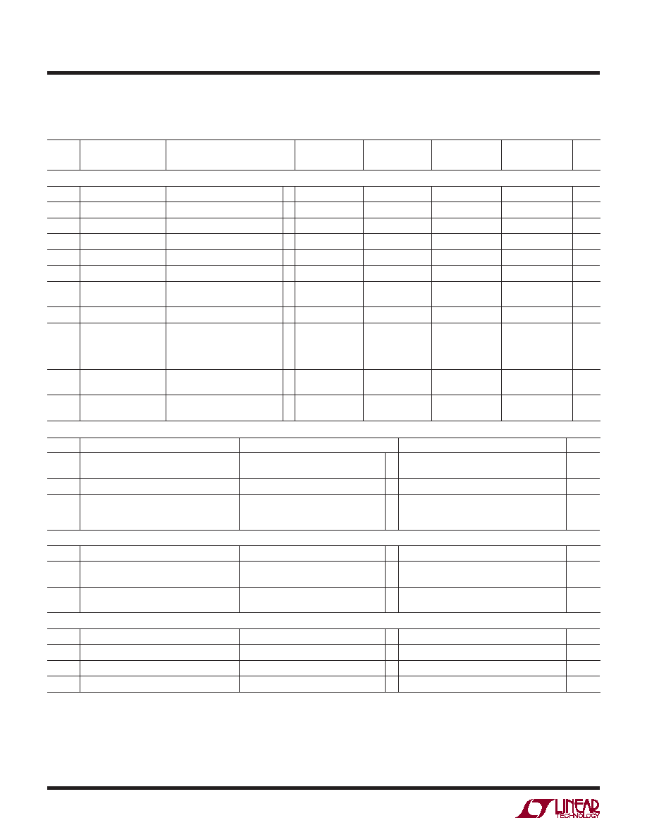
electrical characteristics
SYMBOL PARAMETER
CONDITIONS
LTC2630-8
LTC2630-10
LTC2630-12
LTC2630A-12
UNITS
MIN TYP MAX MIN TYP MAX MIN TYP MAX MIN TYP MAX
DC Performance
Resolution
l
8
10
12
Bits
Monotonicity
VCC = 5V, Internal Ref. (Note 4) l 8
10
12
Bits
DNL
Differential Nonlinearity VCC = 5V, Internal Ref. (Note 4) l
±0.5
±1
LSB
INL
Integral Nonlinearity
VCC = 5V, Internal Ref. (Note 4) l
±0.05 ±0.5
±0.2
±1
±2
±0.5
±1
LSB
ZSE
Zero Scale Error
VCC = 5V, Internal Ref., Code = 0 l
0.5
5
0.5
5
0.5
5
0.5
5
mV
VOS
Offset Error
VCC = 5V, Internal Ref. (Note 5) l
±0.5
±5
±0.5
±5
±0.5
±5
±0.5
±5
mV
VOSTC VOS Temperature
Coefficient
VCC = 5V, Internal Ref. (Note 5)
±10
V/°C
FSE
Full Scale Error
VCC = 5V, Internal Ref.
l
±0.2 ±0.8
%FSR
VFSTC
Full Scale Voltage
Temperature
Coefficient
VCC = 5V, Internal Ref. (Note 10)
C-Grade
I-Grade
H-Grade
±10
ppm/°C
Load Regulation
VCC = 5V ±10%, Internal Ref.,
Mid-Scale, –10mA ≤ IOUT ≤ 10mA
l
0.006 0.01
0.025 0.04
0.10 0.16
LSB/
mA
ROUT
DC Output Impedance VCC = 5V ±10%, Internal Ref.,
Mid-Scale, –10mA ≤ IOUT ≤ 10mA
l
0.1
0.156
0.1
0.156
0.1
0.156
0.1
0.156
Ω
The l denotes the specifications which apply over the full operating
temperature range, otherwise specifications are at TA = 25°C. VCC = 4.5V to 5.5V, VOUT unloaded unless otherwise specified.
LTC2630-HM12/-HM10/-HM8/-HZ12/-HZ10/-HZ8, LTC2630A-HM12/-HZ12 (VFS = 4.096V)
SYMBOL PARAMETER
CONDITIONS
MIN
TYP
MAX
UNITS
VOUT
DAC Output Span
Supply as Reference
Internal Reference
0V to VCC
0V to 4.096
V
PSR
Power Supply Rejection
VCC = 5V ±10%
–80
dB
ISC
Short Circuit Output Current (Note 6)
Sinking
Sourcing
VFS = VCC = 5.5V
Zero Scale; VOUT Shorted to VCC
Full Scale; VOUT Shorted to GND
l
27
–28
50
–50
mA
Power Supply
VCC
Power Supply Voltage
For Specified Performance
l
4.5
5.5
V
ICC
Supply Current (Note 7)
VCC = 5V, Supply as Reference
VCC = 5V, Internal Reference
l
180
200
260
280
A
ISD
Supply Current in Power-Down Mode
(Note 7)
VCC = 5V, C-Grade, I-Grade
VCC = 5V, H-Grade
l
0.36
1.8
5
A
Digital I/O
VIH
Digital Input High Voltage
l
2.4
V
VIL
Digital Input Low Voltage
l
0.8
V
ILK
Digital Input Leakage
VIN = GND to VCC
l
±1
A
CIN
Digital Input Capacitance
(Note 8)
l
2.5
pF
发布紧急采购,3分钟左右您将得到回复。
相关PDF资料
LTC2642IDD-16#PBF
IC DAC 16BIT VOUT 10-DFN
LTC2704IGW-16#PBF
IC DAC 16BIT QUAD VOUT 44-SSOP
LTC2751AIUHF-16#PBF
IC DAC 16BIT CUR OUT 38-QFN
LTC2752ACLX#PBF
IC DAC 16BIT DUAL CUR OUT 48LQFP
LTC2753AIUK-16#TRPBF
IC DAC 16BIT DUAL 48-QFN
LTC2754AIUKG-16#PBF
IC DAC 16BIT QUAD IOUT 52-QFN
LTC2755AIUP-16#PBF
IC DAC 16BIT CUR OUT 64-QFN
LTC2757ACLX#PBF
IC DAC 18BIT PAR 48LQFP
相关代理商/技术参数
LTC2630HSC6-LZ8#PBF
制造商:Linear Technology 功能描述:8BIT DAC R/R INT REF SMD SC70-6 制造商:Linear Technology 功能描述:8BIT DAC R/R, INT REF, SMD, SC70-6
LTC2630HSC6-LZ8#TRMPBF
功能描述:IC DAC 8BIT R-R SC70-6 RoHS:是 类别:集成电路 (IC) >> 数据采集 - 数模转换器 系列:- 产品培训模块:Lead (SnPb) Finish for COTS
Obsolescence Mitigation Program 标准包装:58 系列:- 设置时间:6µs 位数:8 数据接口:并联 转换器数目:4 电压电源:双 ± 功率耗散(最大):640mW 工作温度:-40°C ~ 85°C 安装类型:表面贴装 封装/外壳:24-SSOP(0.209",5.30mm 宽) 供应商设备封装:24-SSOP 包装:管件 输出数目和类型:4 电压,单极;4 电压,双极 采样率(每秒):*
LTC2630HSC6-LZ8#TRPBF
功能描述:IC DAC 8BIT R-R SC70-6 RoHS:是 类别:集成电路 (IC) >> 数据采集 - 数模转换器 系列:- 产品培训模块:Data Converter Fundamentals
DAC Architectures 设计资源:Unipolar, Precision DC Digital-to-Analog Conversion using AD5450/1/2/3 8-14-Bit DACs (CN0052)
Precision, Bipolar, Configuration for AD5450/1/2/3 8-14bit Multiplying DACs (CN0053)
AC Signal Processing Using AD5450/1/2/3 Current Output DACs (CN0054)
Programmable Gain Element Using AD5450/1/2/3 Current Output DAC Family (CN0055)
Single Supply Low Noise LED Current Source Driver Using a Current Output DAC in the Reverse Mode (CN0139) 标准包装:10,000 系列:- 设置时间:- 位数:12 数据接口:DSP,MICROWIRE?,QSPI?,串行,SPI? 转换器数目:1 电压电源:单电源 功率耗散(最大):- 工作温度:-40°C ~ 125°C 安装类型:表面贴装 封装/外壳:SOT-23-8 薄型,TSOT-23-8 供应商设备封装:TSOT-23-8 包装:带卷 (TR) 输出数目和类型:1 电流,单极;1 电流,双极 采样率(每秒):2.7M
LTC2630ISC6-HM10#TRMPBF
功能描述:IC DAC 10BIT R-R SC70-6 RoHS:是 类别:集成电路 (IC) >> 数据采集 - 数模转换器 系列:- 产品培训模块:Lead (SnPb) Finish for COTS
Obsolescence Mitigation Program 标准包装:58 系列:- 设置时间:6µs 位数:8 数据接口:并联 转换器数目:4 电压电源:双 ± 功率耗散(最大):640mW 工作温度:-40°C ~ 85°C 安装类型:表面贴装 封装/外壳:24-SSOP(0.209",5.30mm 宽) 供应商设备封装:24-SSOP 包装:管件 输出数目和类型:4 电压,单极;4 电压,双极 采样率(每秒):*
LTC2630ISC6-HM10#TRPBF
功能描述:IC DAC 10BIT R-R SC70-6 RoHS:是 类别:集成电路 (IC) >> 数据采集 - 数模转换器 系列:- 产品培训模块:Data Converter Fundamentals
DAC Architectures 设计资源:Unipolar, Precision DC Digital-to-Analog Conversion using AD5450/1/2/3 8-14-Bit DACs (CN0052)
Precision, Bipolar, Configuration for AD5450/1/2/3 8-14bit Multiplying DACs (CN0053)
AC Signal Processing Using AD5450/1/2/3 Current Output DACs (CN0054)
Programmable Gain Element Using AD5450/1/2/3 Current Output DAC Family (CN0055)
Single Supply Low Noise LED Current Source Driver Using a Current Output DAC in the Reverse Mode (CN0139) 标准包装:10,000 系列:- 设置时间:- 位数:12 数据接口:DSP,MICROWIRE?,QSPI?,串行,SPI? 转换器数目:1 电压电源:单电源 功率耗散(最大):- 工作温度:-40°C ~ 125°C 安装类型:表面贴装 封装/外壳:SOT-23-8 薄型,TSOT-23-8 供应商设备封装:TSOT-23-8 包装:带卷 (TR) 输出数目和类型:1 电流,单极;1 电流,双极 采样率(每秒):2.7M
LTC2630ISC6-HM12#PBF
制造商:Linear Technology 功能描述:IC 12BIT DAC R/R INT REF SC70-6 制造商:Linear Technology 功能描述:MS-DAC/Industrial, Cut Tape 12-bit Vout DAC SC70
LTC2630ISC6-HM12#TRMPBF
功能描述:IC DAC 12BIT R-R SC70-6 RoHS:是 类别:集成电路 (IC) >> 数据采集 - 数模转换器 系列:- 产品培训模块:Lead (SnPb) Finish for COTS
Obsolescence Mitigation Program 标准包装:58 系列:- 设置时间:6µs 位数:8 数据接口:并联 转换器数目:4 电压电源:双 ± 功率耗散(最大):640mW 工作温度:-40°C ~ 85°C 安装类型:表面贴装 封装/外壳:24-SSOP(0.209",5.30mm 宽) 供应商设备封装:24-SSOP 包装:管件 输出数目和类型:4 电压,单极;4 电压,双极 采样率(每秒):*
LTC2630ISC6-HM12#TRPBF
功能描述:IC DAC 12BIT R-R SC70-6 RoHS:是 类别:集成电路 (IC) >> 数据采集 - 数模转换器 系列:- 产品培训模块:Data Converter Fundamentals
DAC Architectures 设计资源:Unipolar, Precision DC Digital-to-Analog Conversion using AD5450/1/2/3 8-14-Bit DACs (CN0052)
Precision, Bipolar, Configuration for AD5450/1/2/3 8-14bit Multiplying DACs (CN0053)
AC Signal Processing Using AD5450/1/2/3 Current Output DACs (CN0054)
Programmable Gain Element Using AD5450/1/2/3 Current Output DAC Family (CN0055)
Single Supply Low Noise LED Current Source Driver Using a Current Output DAC in the Reverse Mode (CN0139) 标准包装:10,000 系列:- 设置时间:- 位数:12 数据接口:DSP,MICROWIRE?,QSPI?,串行,SPI? 转换器数目:1 电压电源:单电源 功率耗散(最大):- 工作温度:-40°C ~ 125°C 安装类型:表面贴装 封装/外壳:SOT-23-8 薄型,TSOT-23-8 供应商设备封装:TSOT-23-8 包装:带卷 (TR) 输出数目和类型:1 电流,单极;1 电流,双极 采样率(每秒):2.7M